- 您现在的位置:买卖IC网 > Sheet目录345 > MT48H32M16LFB4-75B IT:C (Micron Technology Inc)IC SDRAM 512MB 54VFBGA
�� �
�
�512Mb:� 32� Meg� x� 16,� 16� Meg� x� 32� Mobile� SDRAM�
�READ� Operation�
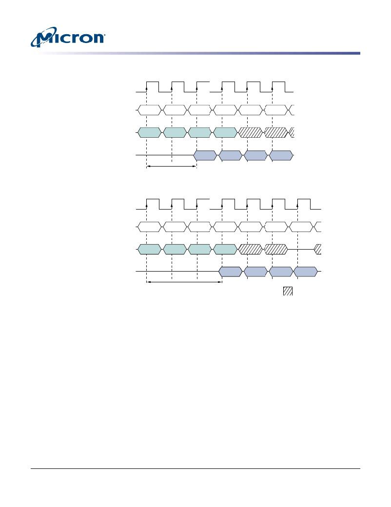
�Figure� 18:� Random� READ� Accesses�
�T0�
�T1�
�T2�
�T3�
�T4�
�T5�
�CLK�
�Command�
�Address�
�DQ�
�READ�
�Bank,�
�Col� n�
�READ�
�Bank,�
�Col� a�
�READ�
�Bank,�
�Col� x�
�D� OUT�
�n�
�READ�
�Bank,�
�Col� m�
�D� OUT�
�a�
�NOP�
�D� OUT�
�x�
�NOP�
�D� OUT�
�m�
�CL� =� 2�
�T0�
�T1�
�T2�
�T3�
�T4�
�T5�
�T6�
�CLK�
�Command�
�READ�
�READ�
�READ�
�READ�
�NOP�
�NOP�
�NOP�
�Address�
�Bank,�
�Col� n�
�Bank,�
�Col� a�
�Bank,�
�Col� x�
�Bank,�
�Col� m�
�DQ�
�D� OUT�
�n�
�D� OUT�
�a�
�D� OUT�
�x�
�D� OUT�
�m�
�CL� =� 3�
�Don’t� Care�
�Note:�
�1.� Each� READ� command� can� be� issued� to� any� bank.� DQM� is� LOW.�
�Data� from� any� READ� burst� can� be� truncated� with� a� subsequent� WRITE� command,� and�
�data� from� a� fixed-length� READ� burst� can� be� followed� immediately� by� data� from� a�
�WRITE� command� (subject� to� bus� turnaround� limitations).� The� WRITE� burst� can� be� ini-�
�tiated� on� the� clock� edge� immediately� following� the� last� (or� last� desired)� data� element�
�from� the� READ� burst,� provided� that� I/O� contention� can� be� avoided.� In� a� given� system�
�design,� there� is� a� possibility� that� the� device� driving� the� input� data� will� go� Low-Z� before�
�the� DQ� go� High-Z.� In� this� case,� at� least� a� single-cycle� delay� should� occur� between� the�
�last� read� data� and� the� WRITE� command.�
�The� DQM� input� is� used� to� avoid� I/O� contention,� as� shown� in� Figure� 19� (page� 50)� and�
�Figure� 20� (page� 51).� The� DQM� signal� must� be� asserted� (HIGH)� at� least� two� clocks� prior�
�to� the� WRITE� command� (DQM� latency� is� two� clocks� for� output� buffers)� to� suppress� da-�
�ta-out� from� the� READ.� After� the� WRITE� command� is� registered,� the� DQ� will� go� to� High-Z�
�(or� remain� High-Z),� regardless� of� the� state� of� the� DQM� signal,� provided� the� DQM� was�
�active� on� the� clock� just� prior� to� the� WRITE� command� that� truncated� the� READ� com-�
�mand.� If� not,� the� second� WRITE� will� be� an� invalid� WRITE.� For� example,� if� DQM� was�
�LOW� during� T4,� then� the� WRITEs� at� T5� and� T7� would� be� valid,� and� the� WRITE� at� T6�
�would� be� invalid.�
�PDF:� 09005aef8459c827�
�512mb_mobile_sdram_y67m_at.pdf� –� Rev.� B� 3/11� EN�
�49�
�Micron� Technology,� Inc.� reserves� the� right� to� change� products� or� specifications� without� notice.�
�?� 2011� Micron� Technology,� Inc.� All� rights� reserved.�
�发布紧急采购,3分钟左右您将得到回复。
相关PDF资料
MT48H8M16LFB4-75 IT:K TR
IC SDRAM 128MBIT 133MHZ 54VFBGA
MTC100-JA2-P34
CONTACT INSERT PIN
MX841BE
IC CONVERTER WHITE LED 8-SOIC
MXHV9910BTR
IC LED DRIVER HIGH BRIGHT 8-SOIC
MXN12FB12F
MOTOR BRUSHED DC 12V 2922RPM
MXN13FB08B1
MOTOR BRUSHED DC 8V 4714RPM
N01L63W2AB25I
IC SRAM ASYNC 1MBIT ULP 48-BGA
N01L63W3AB25I
IC SRAM 1MBIT 3V LP 48-BGA
相关代理商/技术参数